Meditating with microprocessors
- Artificial Intelligence based Hardware(Microprocessor) tuning: Implementing a very simple idea (part-1)
- A crashcourse in Microarchitecture and Linux CPUIDLE interface (part-2)
- Trading off power for UltraLowLatency (part-3)
- Artificial Intelligence guided Predictive MicroProcessor tuning (part-4)
- Introduction
- Is there a solution?
- Is there a smarter solution?: Artificial Intelligence model based proactive decision making
- Recognizing the pattern
- Transformer as the backbone
- Transfer Learning inspiration from NLP
- Fine tuning pre-trained networks
- Artificial Intelligence model based proactive and predictive decision making
- The Final Cut
- Summary
- Appendix:Tools of the trade (part-5)
Introduction
The current article is part of a bigger series titled Meditating-with-microprocessors, in which I demonstrate the use of Artificial Intelligence to tune microprocessors for Ultra Low Latency and Realtime loads. There are 5 parts to the series, Meditating with Microprocessors: An essentially simple idea(part-1) , A crashcourse in Microarchitecture and Linux CPUIDLE interface(part-2), Trading off power for UltraLowLatency (part-3) , Artificial Intelligence guided Predictive MicroProcessor tuning (part-4), Appendix:Tools of the trade (part-5).
In the current article I lay the technical groundwork for later articles in the series to build on. The terms and technologies I’ll be using later must be understood really well. So we look at 3 concepts primarily.
- Firstly, the architecture of a modern microprocessor in short, really really short. Just enough to make a mental model of the microprocessor to work with.
- Secondly, How does the software(Linux) interface with the microprocessor. Again, just enough to make sense of the data we gather from the CPU using various UltraLowLatency profilers and tracers.
- Thirdly, help programmers like you to get started quickly, explore further, and help us.
MicroProcessor Components
- Core: The modules/agents that compute are called the cores in a CPU. They may be general-purpose CPU cores or special purpose GPGPU cores. Cores take instructions from a software program and execute them loads, stores, “arithmetic and control flow”.
- Cache: Caches frequently used data so that expensive memory access can be avoided. There is usually a hierarchy of multiple levels of cache. L1 and L2 are quick access (static RAM chips) small in size. L3 and L4, slower to access (dynamic RAM chips) but comparatively larger in size. Also, L3 and L4 are usually on the die as the core.
- On-chip-fabric: Interconnects exist on the CPU dies that are commonly called on-die or on-chip fabrics. These are not to be confused with fabrics that connect multiple CPU dies together at the data center level.
- Memory controller: Memory controllers provide an interface to main memory (DDR in many recent processor generations).
- PCIe: PCIe provides a mechanism to connect external devices such as network cards into the CPU.
- Chipset: The chipset can be thought of as a support entity to the CPU. In addition to supporting the boot process, it can also provide additional capabilities such as PCIe, hard drive access, networking, and manageability. Chipset functionality is integrated into the same die or package as the cores in the microserver space.
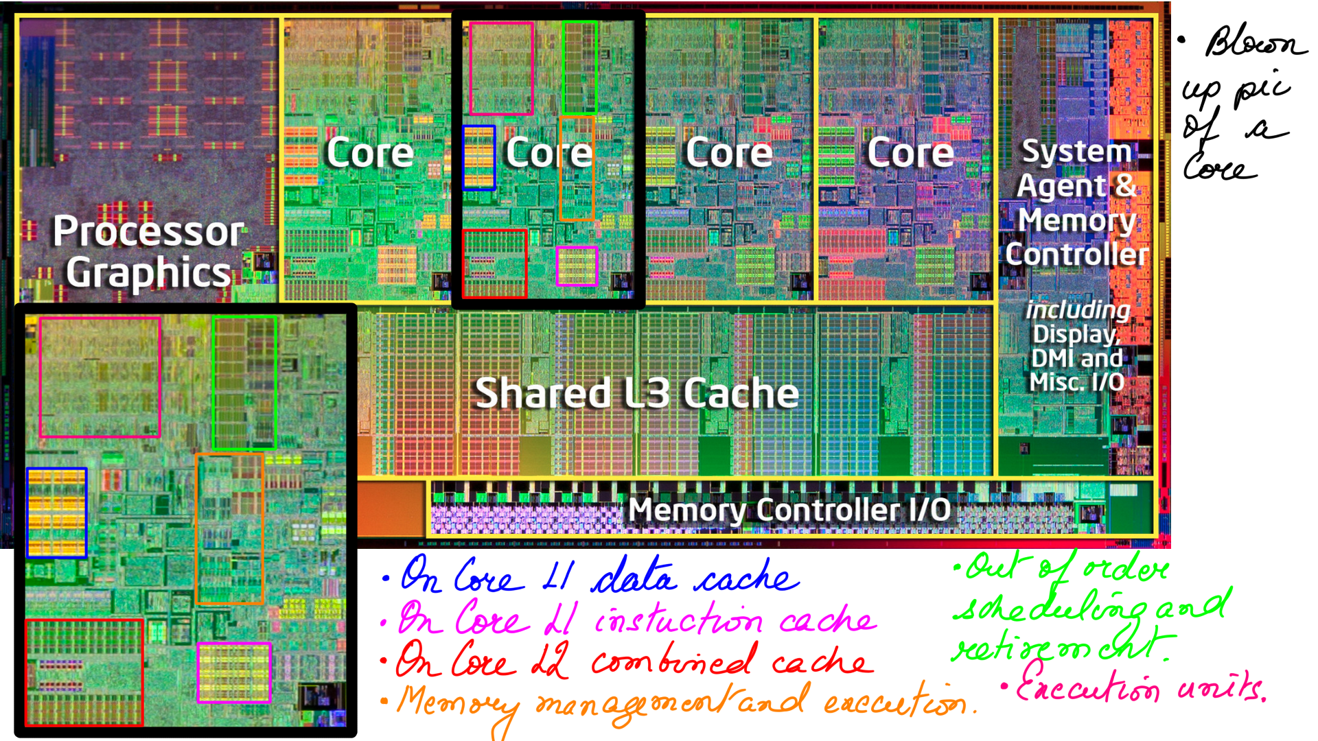
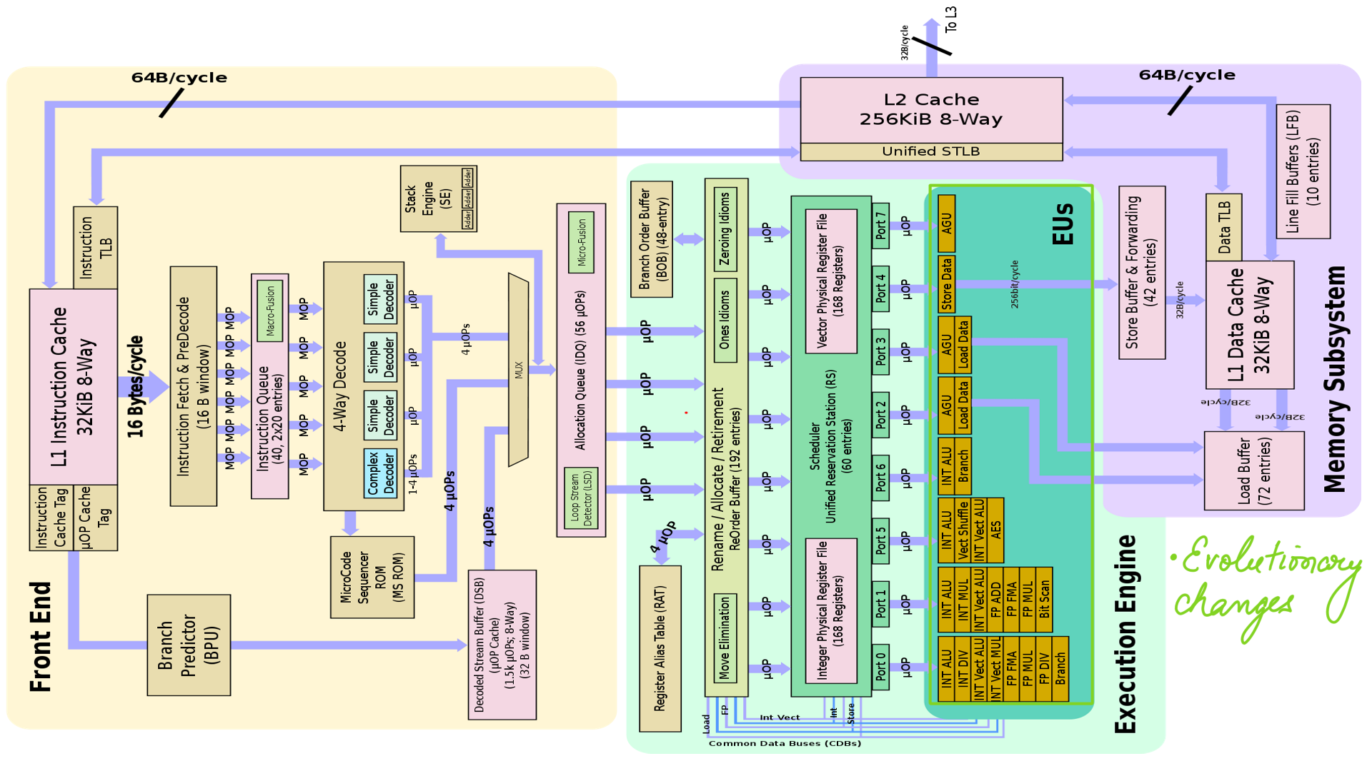
Core
Full-length books and courses have been dedicated to microarchitecture, so to illustrate the idea in a few pictures is foolhardy, to say the least. The complexity of this subject is second to none. And yet, I’ll give it a try, because the essence is not that difficult and worth understanding. Also, I have marked some links that do an excellent treatment of the subject in the references below. The first thing we look at is the flow of instruction and data inside the core at a relatively high level.
Cores can be designed for general purpose usage where they work well for a wide range of workloads. The trade of with general purpose cores is a relatively higher cost of design and construction. As a result, there are special-purpose cores, that trade-off floating-point performance, or 64-bit precision e.t.c. for smaller form factor or cost. In this section, we look at general-purpose cores. Also, we look at Sandy Bridge as it is relatively modern and Intel makes evolutionary changes moving forward to Haswell and *Lake pipelines.
Follow the color code.
- Core: Identifying various modules/units in the core.
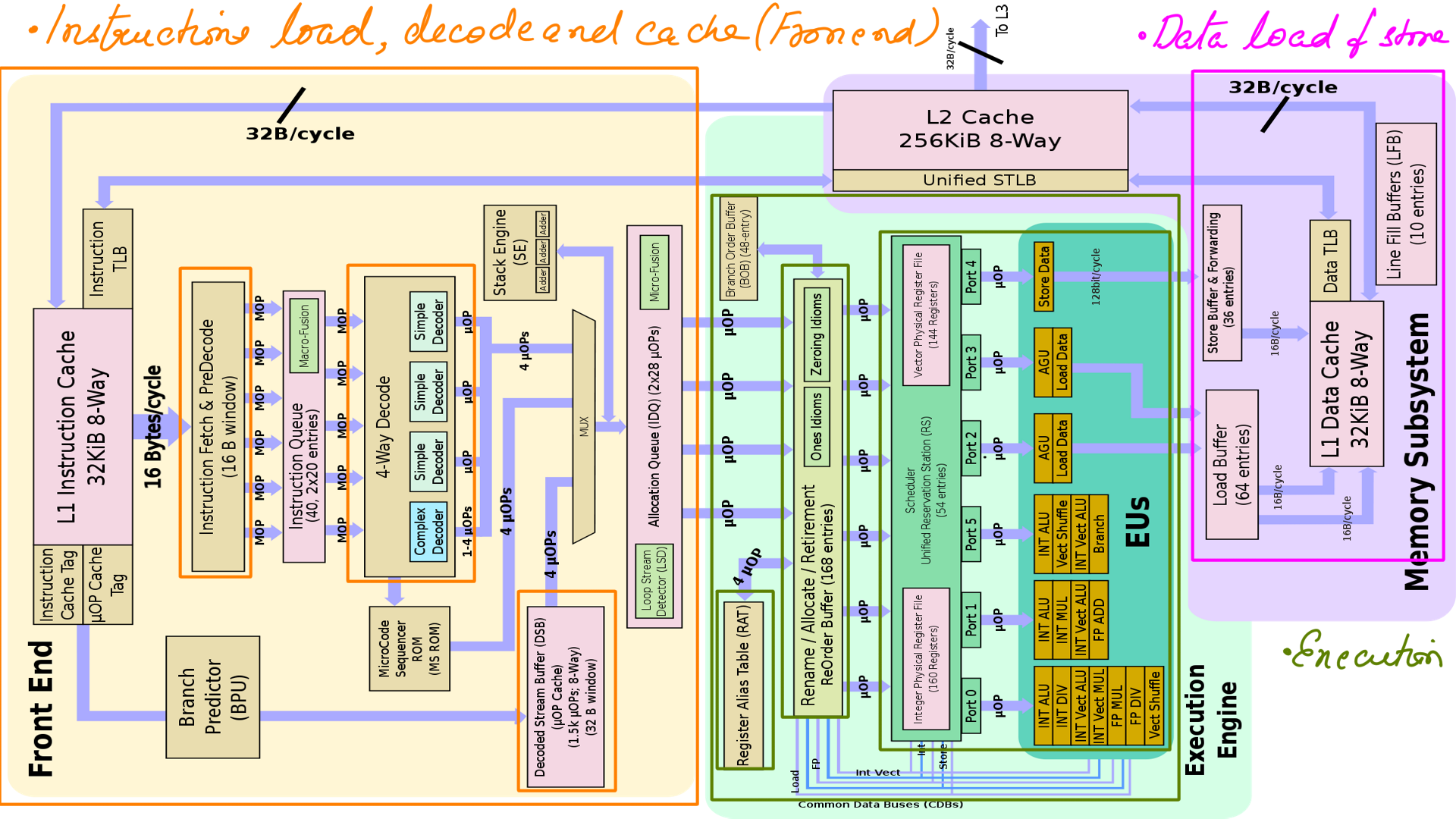
Sandy Bridge Pipeline:Frontend(Instruction load, decode, cache)
This details the frontend of the core. How the INSTRUCTIONS(NOT DATA) are loaded, decoded and cached. They have been designed in such a way that multiple μop(micro-operations) are available for execution at every cycle to increase parallelism.
- Instruction fetch(figure-2(yellow)):Instruction codes are fetched from the code cache(L1i-cache) in aligned 16-byte chunks into a double buffer that can hold two 16-byte chunks. The purpose of the double buffer is to make it possible to decode an instruction that crosses a 16-byte boundary.
- Instruction decoding(figure-2(yellow)):This is a very critical stage in the pipeline because it limits the degree of parallelism that can be achieved. We want to fetch more than one instruction per clock cycle, decode more than one instruction per clock cycle, and execute more than one μop per clock cycle in order to gain speed. But decoding instructions in parallel is difficult when instructions have different lengths. You need to decode the first instruction in order to know how long it is and where the second instruction begins before you can start to decode the second instruction. So a simple instruction length decoder would only be able to handle one instruction per clock cycle. There are four decoders, which can handle instructions generating one or more ]=ops(Micro-operation) according to certain patterns.
- Micro-operation Cache(figure-2(yellow)): The decoded μops(Micro-operation) are cached in a μops(Micro-operation) cache after the decoders in Sandy Bridge. This is useful because the limitation of 16 bytes per clock cycle in the fetch/decode units is a serious bottleneck if the average instruction length is more than four bytes. The throughput is doubled to 32 bytes per clock for code that fits into the μop(Micro-operation) cache.
Sandy Bridge Pipeline:Execution
This is where the execution happens. This is the critical source of performance in modern microprocessors. AFAIK, P5 is the first model from Intel that had multiple ports and an out-of-order( also called dynamic execution) scheduler. This scheme is used in most high-performance CPUs. In this scheme, the order of execution of instructions is determined by the availability of data and execution units and not the source order of the program(Thread). What this means is instructions within a thread may be reordered to suit the availability of data and execution units. The capacity(parallelism) of Sandy Bridge’s execution unit is quite high. Many μops have two or three execution ports to choose between and each unit.
- Register Alias Table(RAT)(figure-2(green)): The assembly code references logical/architectural registers(Think of them as place holders). Every logical register has a set of physical registers associated with it. The processor re-maps/transposes this name(for e.g. %rax) to one specific physical register on the fly. The physical registers are opaque and cannot be referenced directly but only via the canonical names.
- Register allocation and renaming(figure-1(green)): Register renaming is controlled by the register alias table (RAT) and the reorder buffer (ROB).
- Execution Units(EU)(figure-2(green)): The Sandy Bridge and Ivy Bridge have six execution ports. Port 0, 1 and 5 are for arithmetic and logic operations (ALU). There are two identical memory read ports on port 2 and 3 where previous processors had only one. Port 4 is for memory write. The memory write unit on port 4 has no address calculation. All write operations use port 2 or 3 for address calculation. The maximum throughput is one unfused μop on each port per clock cycle.
Sandy Bridge Pipeline:Backend (Data load and Store)
- Memory access(figure-2(pink)): The Sandy Bridge has two memory read ports where previous processors have only one. Cache bank conflicts are quite common when the maximum memory bandwidth is utilized.
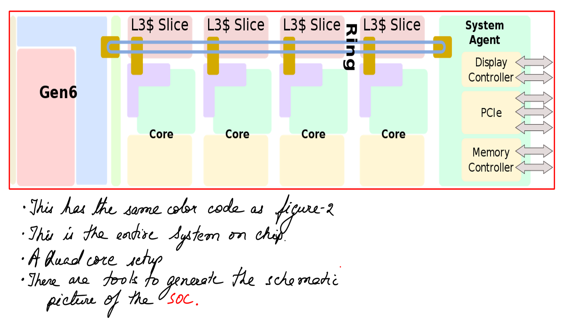
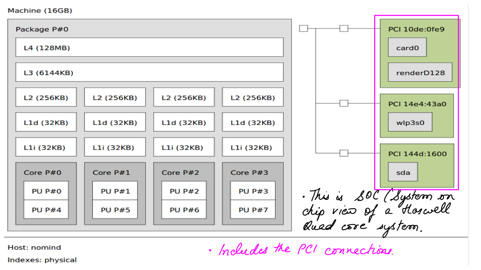
- You can generate the below SOC layout using hwloc lstopo tool
Haswell Pipeline
Intel followed up Sandy and Ivy bridge with Haswell. The Haswell has several important but evolutionary improvements over previous designs. With a few changes, everything has been increased a little bit. Like number of execution units are 8. Compare figure-2 and figure-4 side by side.
- Evolutionary changes in Haswell.
- Evolutionary changes in Haswell. This SOC(System on Chip) view generated by hwloc lstopo tool.
Uncore
All logic that is on the die is referred to as Uncore by Intel. As you may have guessed, that is quite a flimsy definition. But it makes sense because, as we integrate more into the single die or package, it results in a denser design and consumes much less power.
In the Nehalem generation(preceding Sandy bridge ), this included the L3 cache, integrated memory controller, QuickPath Interconnect (QPI; for multi-socket communication), and an interconnect that tied it all together. In the Sandy Bridge generation over and above Sandy Bridge, PCIe was integrated into the CPU uncore.
- L3 cache
- integrated memory controller
- QuickPath Interconnect (QPI; for multi-socket communication)
- interconnect
- PCIe
- Integrated Grafics
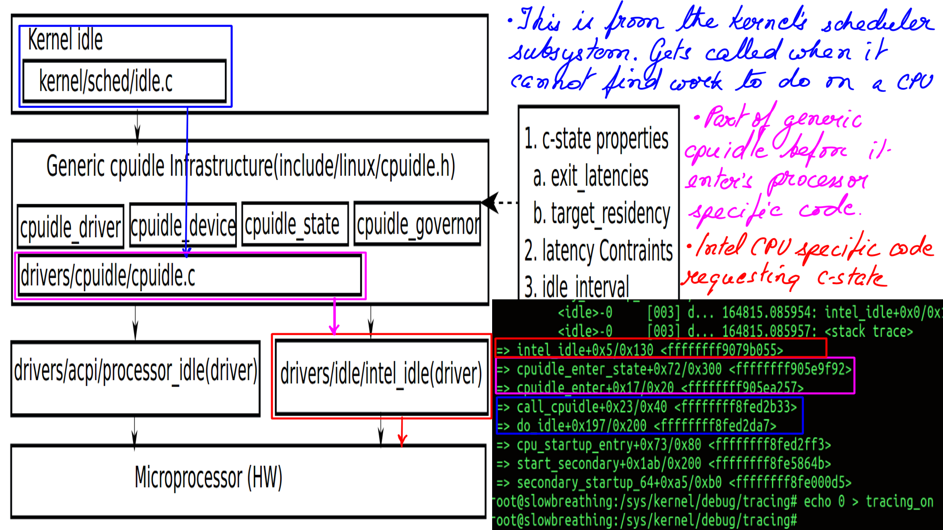
Linux Inteface to CPUIDLE
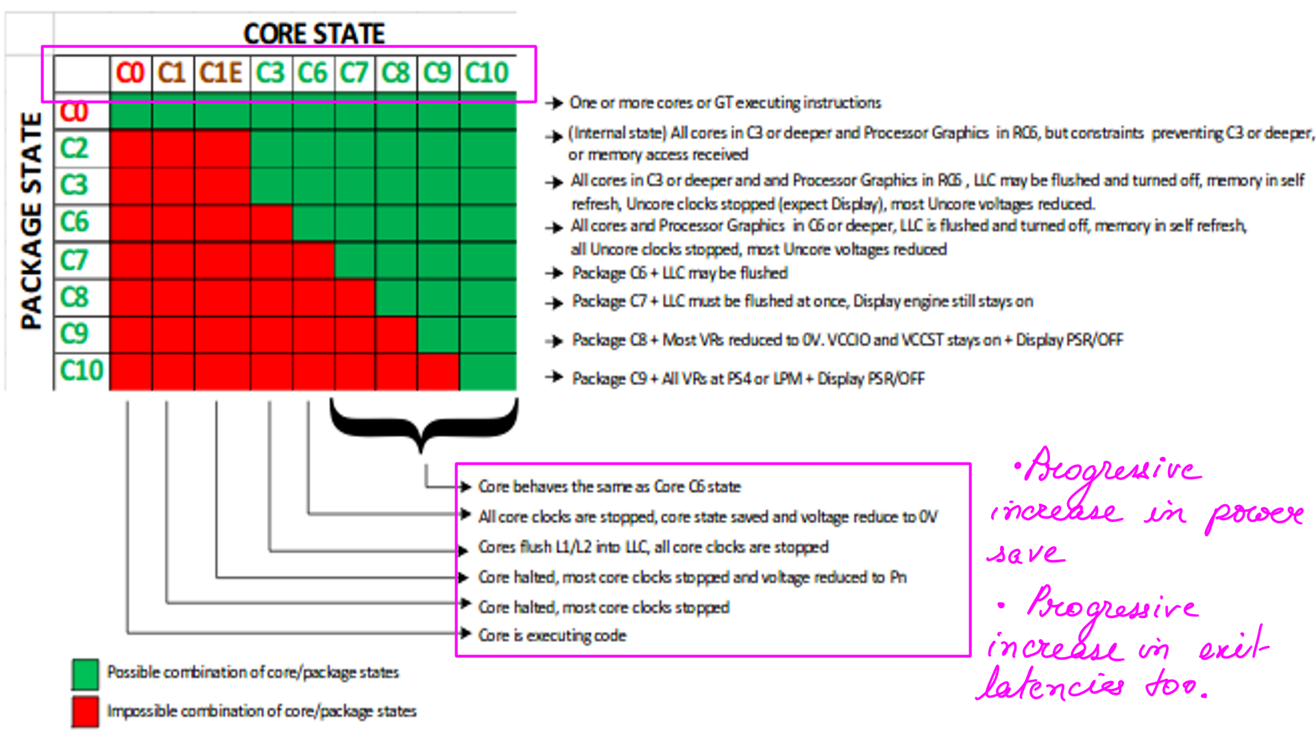
The idea here is to control the deeper c-states( deeper meditative states if you recall ) dynamically at run time. But before that, we need to understand Linux’s interface to a microprocessor. The reason why this is important is that it will help us understand the data gathered by the tracers on the microprocessor’s latency. Understanding this process of interaction allows us to visualize data in more flexible ways. Like mapping c-states to latencies etc.
On most systems the microprocessor is doing some task, editing documents, sending or receiving emails, etc. But what does a microprocessor do when there is nothing to execute. As it turns out, doing nothing is quite complicated. In the olden days idling(doing nothing) was merely the lowest priority thread in a system on a busy spin. Until a new task popped in. Sooner rather than later, someone was going to realize that it is quite inefficient to expend power without any logical work being done. And this is where deeper c-states come in.
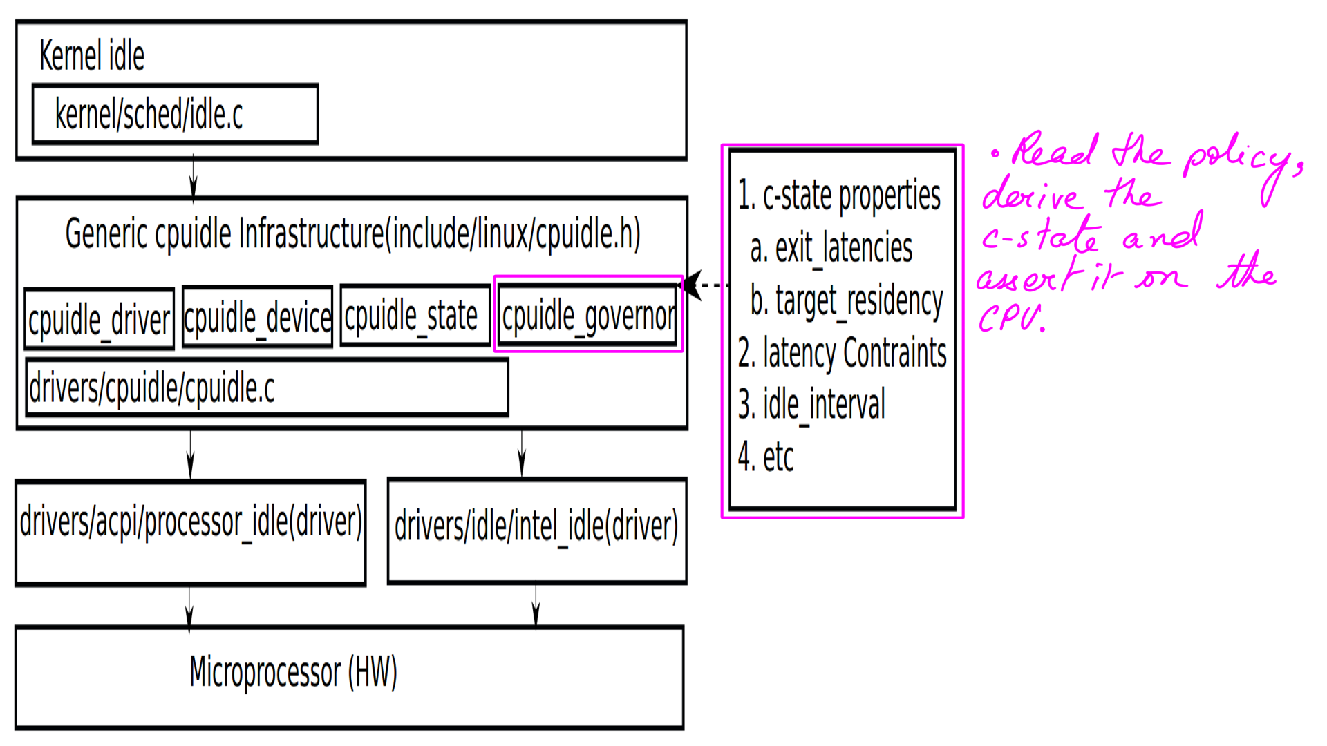
CPUIDLE subsystem
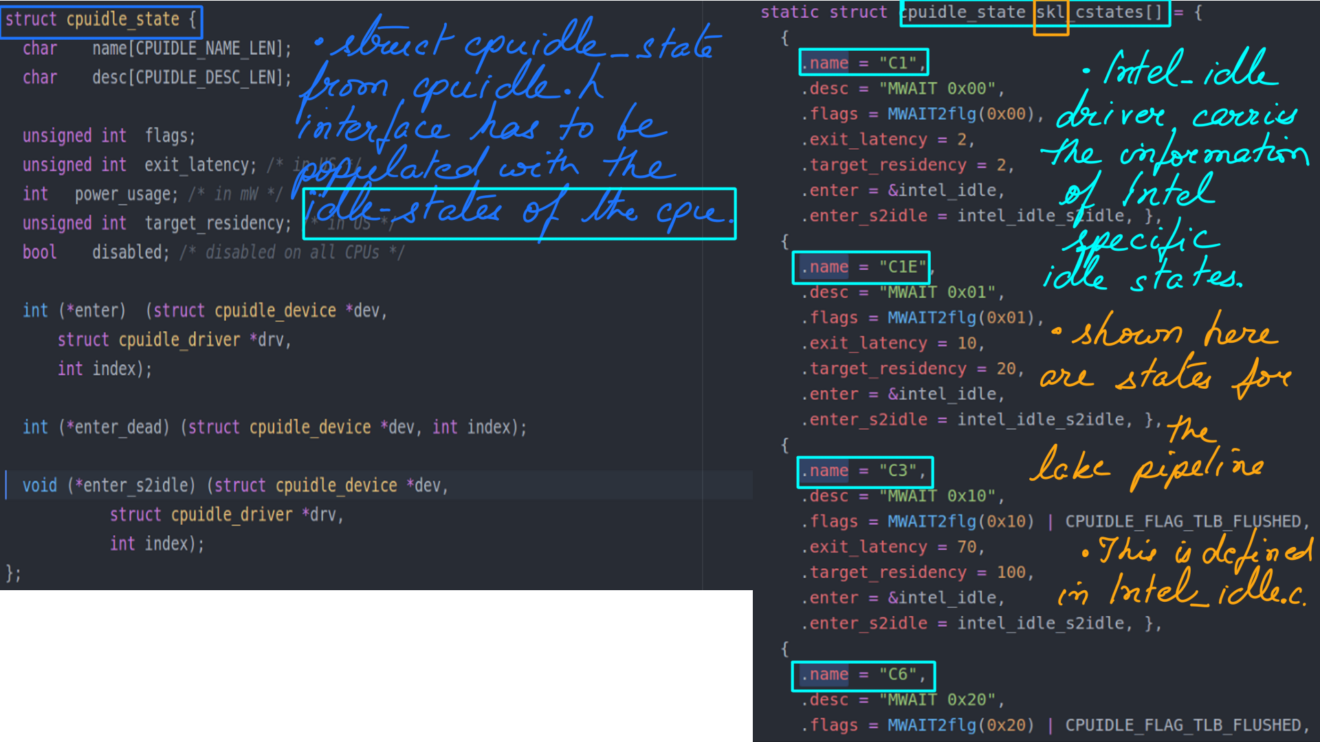
Different processors may have different idle-state characteristics. In fact, even for the same manufacturer, there may be differences from one model to another. “cpuidle.h”(“include/linux/cpuidle.h”) is the generic framework defined for the purpose. “cpuidle.h” acts as an interface to separate platform-independent(rest of the kernel) code from manufacture-dependant(CPU Drivers) ones.
CPUIDLE subsystem:Driver load
The implementation has been handled in 2 different ways.
- For a hardware platform (for e.g. x86), a generic set of idle states may be supported in a manufacture independent way. This is implemented in “acpi_idle”(“drivers/acpi/processor_idle.c”) available at implements this behavior for all/most x86 vendors(Intel/AMD)
- The other choice is to use the Intel driver which is implemented in “intel_idle”(“drivers/idle/intel_idle.c”)
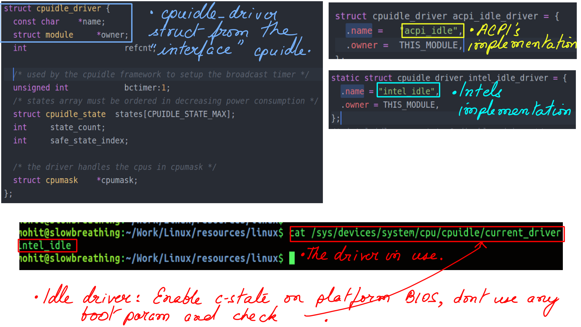
- The figure-9 shows the implementation of “intel_idle” which is implemented in “intel_idle.c”(“drivers/idle/intel_idle.c”)
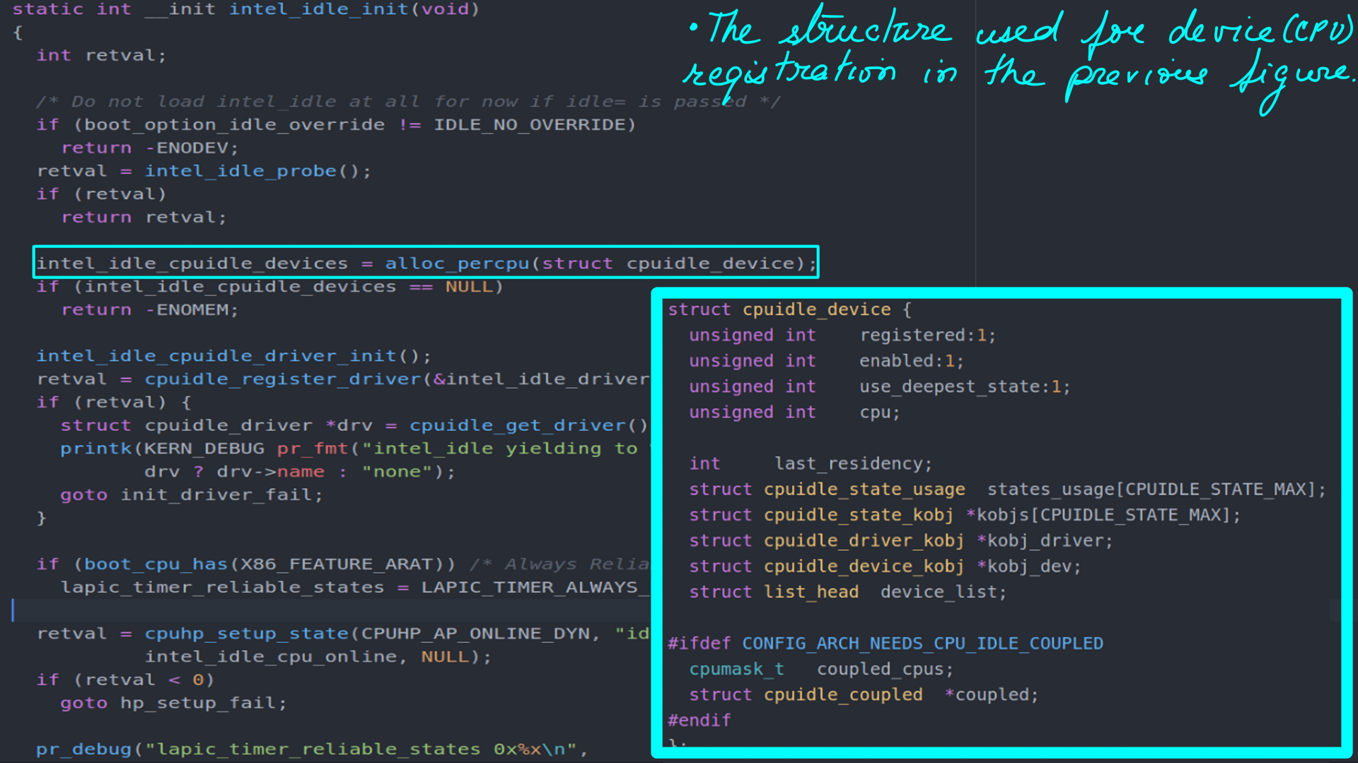
- CPUIDLE driver from Intel initialization function.
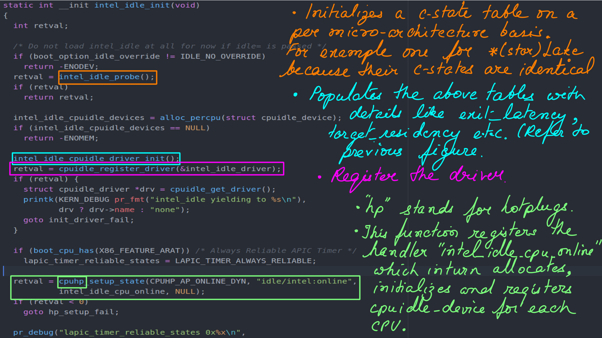
- CPUIDLE driver from Intel initialization function. Figure-(8,9,10,11,12) are to be looked at together to make sense.
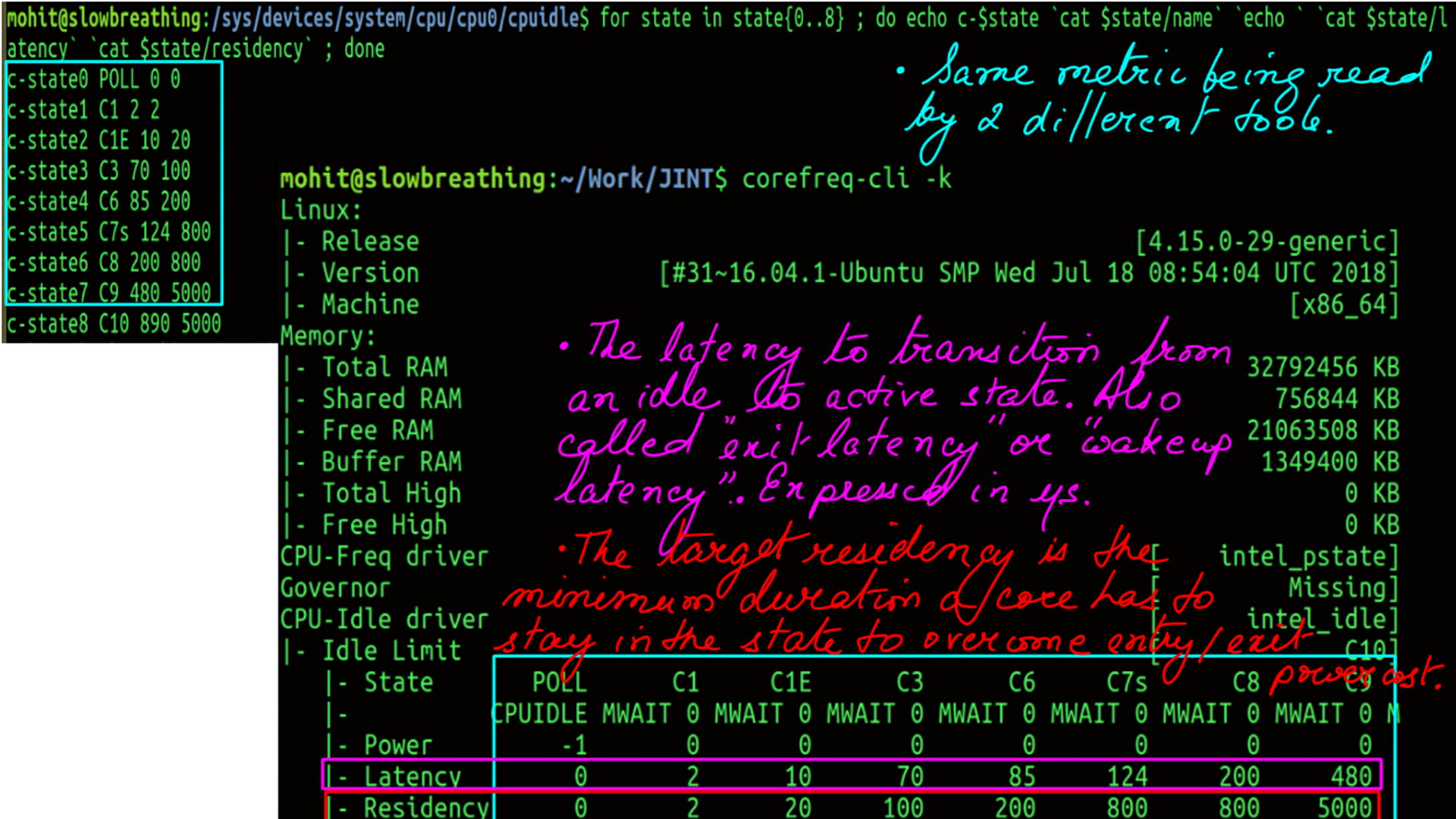
- Finally the result of initialzation can be seen. The idle-states of a modern Intel processor through Linux ‘sysfs’ interface.
CPUIDLE subsystem:Call the Driver
The kernel’s scheduler cannot find a task to run on a CPU so it goes ahead and calls “do_idle”(“kernel/sched/idle.c”). Which idle-state is chosen is a matter of policy, but how then is communicated to the processor is illustrated next.

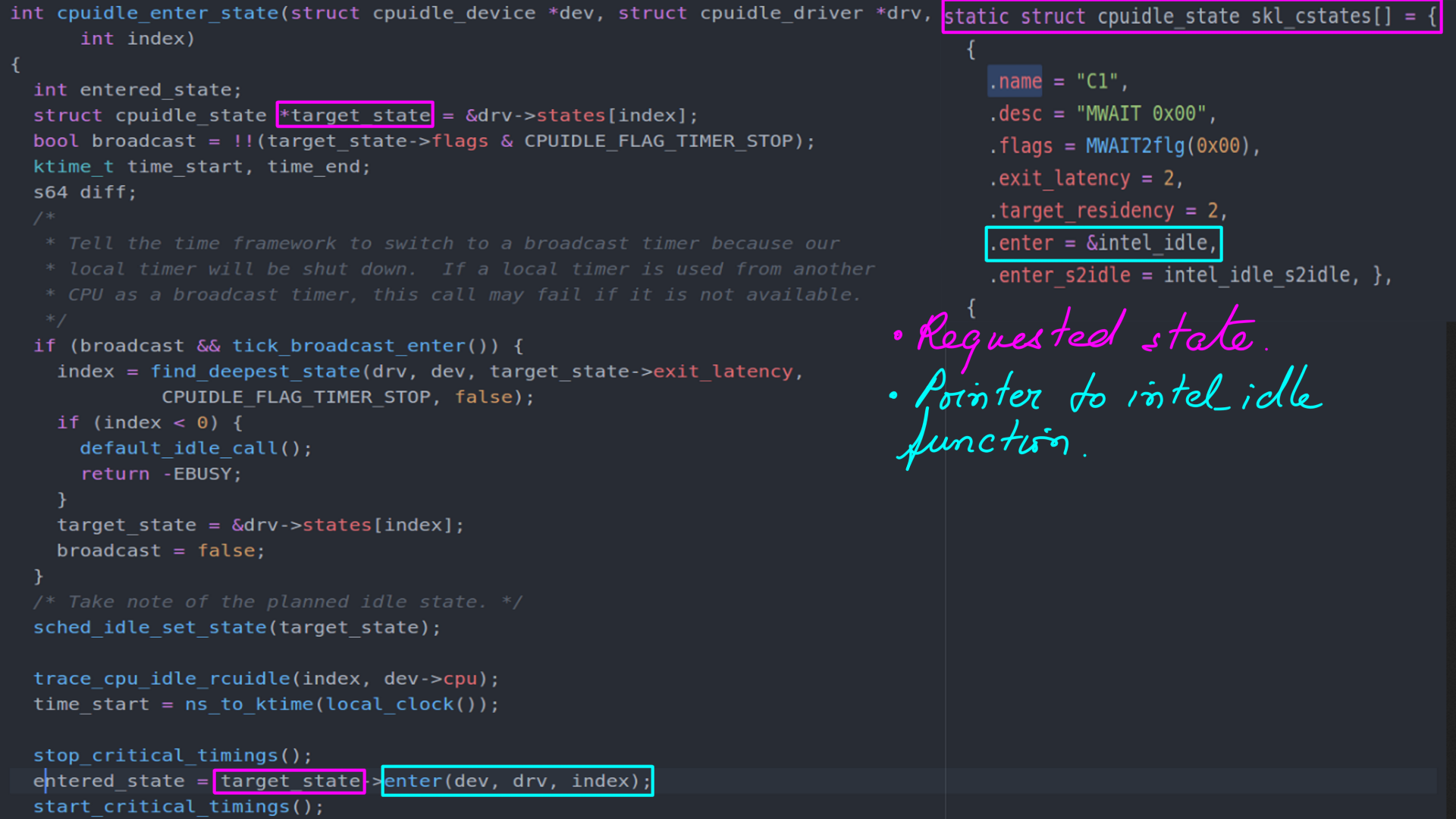
- This one shows the entry to processor specific code of “intel_idle” from “cpuidle_enter_state” (“drivers/cpuidle/cpuidle.c”).
- The target state accessed from driver(struct drv). This state structure is of type “cpuidle_state” shown earlier.
- I traced “sched_idle_set_state” into which “target_state” is getting passed.
- I traced using EBPF. EBPF allows great flexibility in tracing. As you can see I am accessing the struct “cpuidle_state” at run time on a running kernel and printing it out.
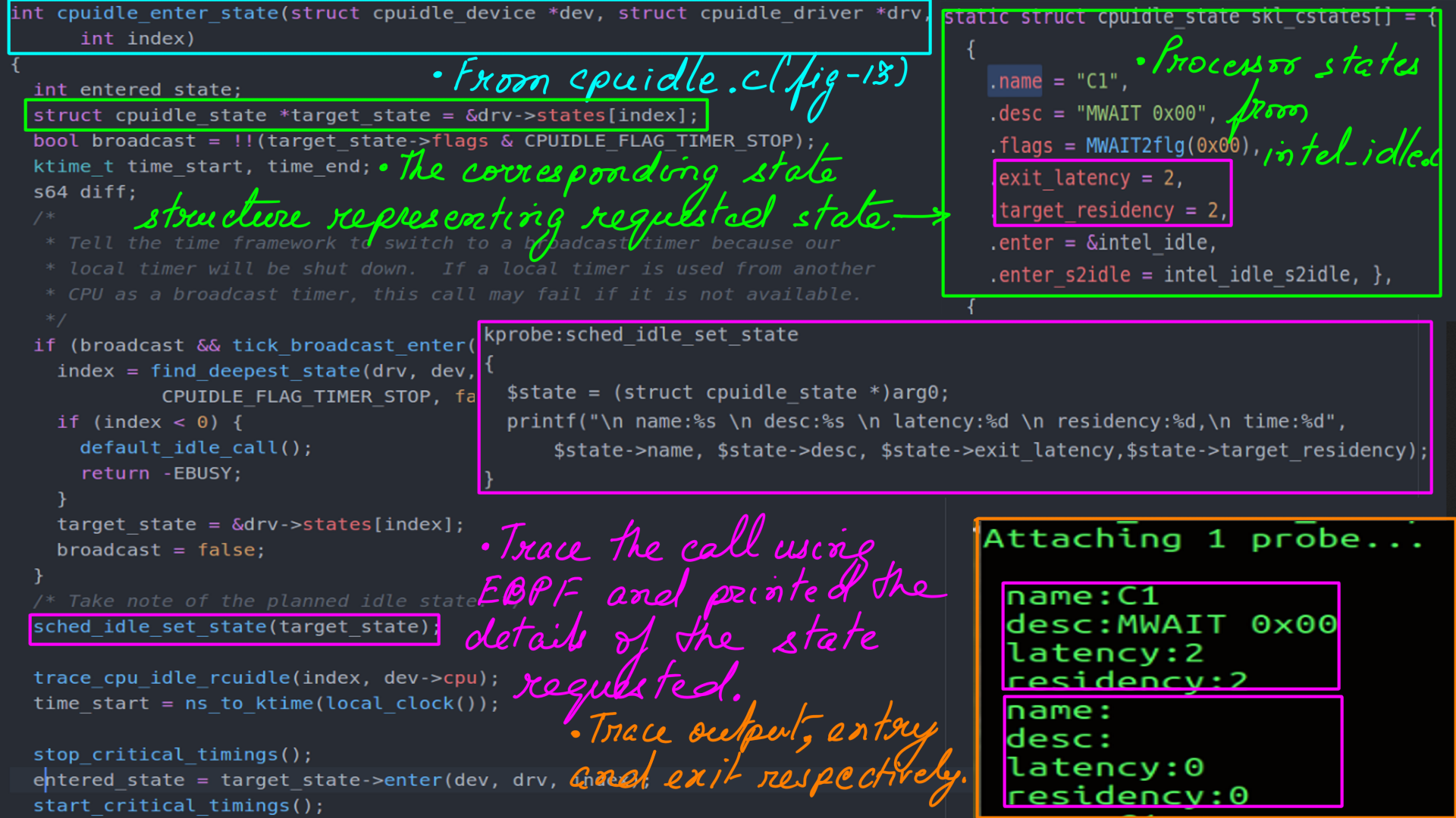
- Finally, call to “intel_idle” from “cpuidle_enter_state” (“drivers/cpuidle/cpuidle.c”).
- Rubber hits the road or the code hits the metal?.
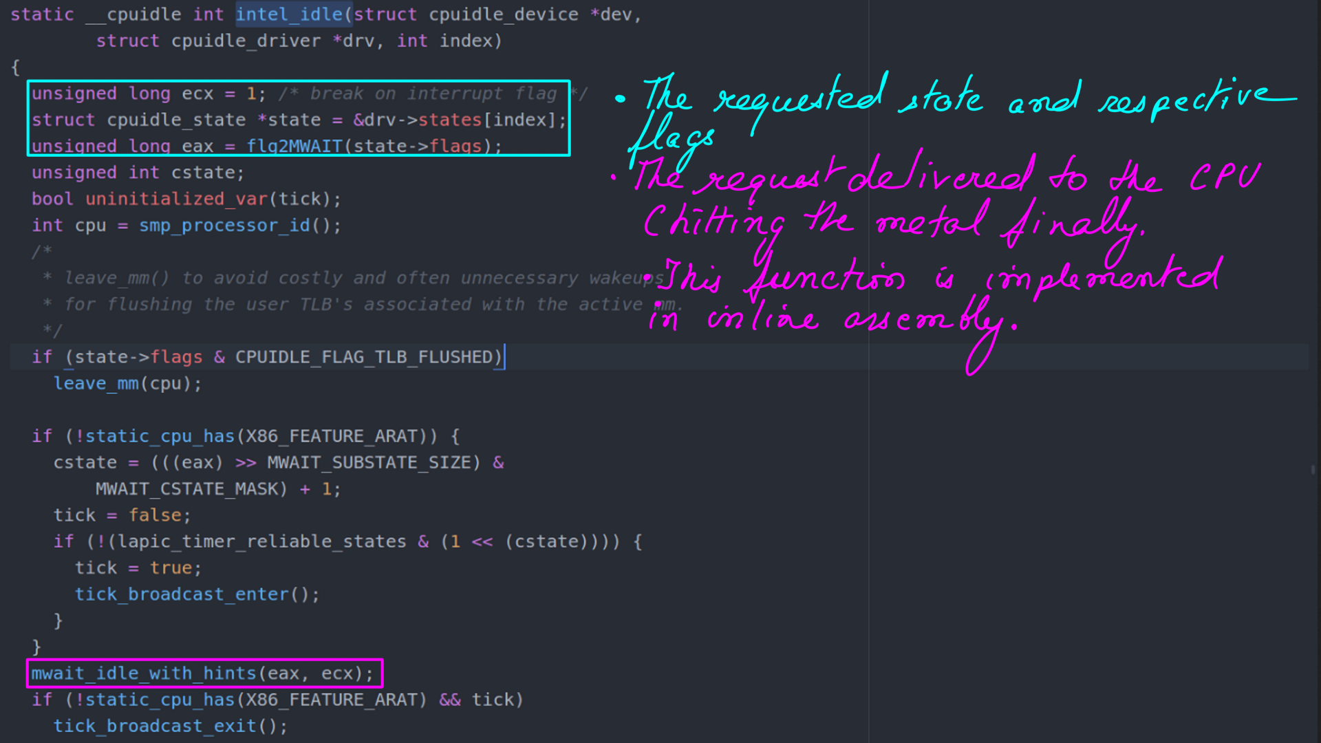
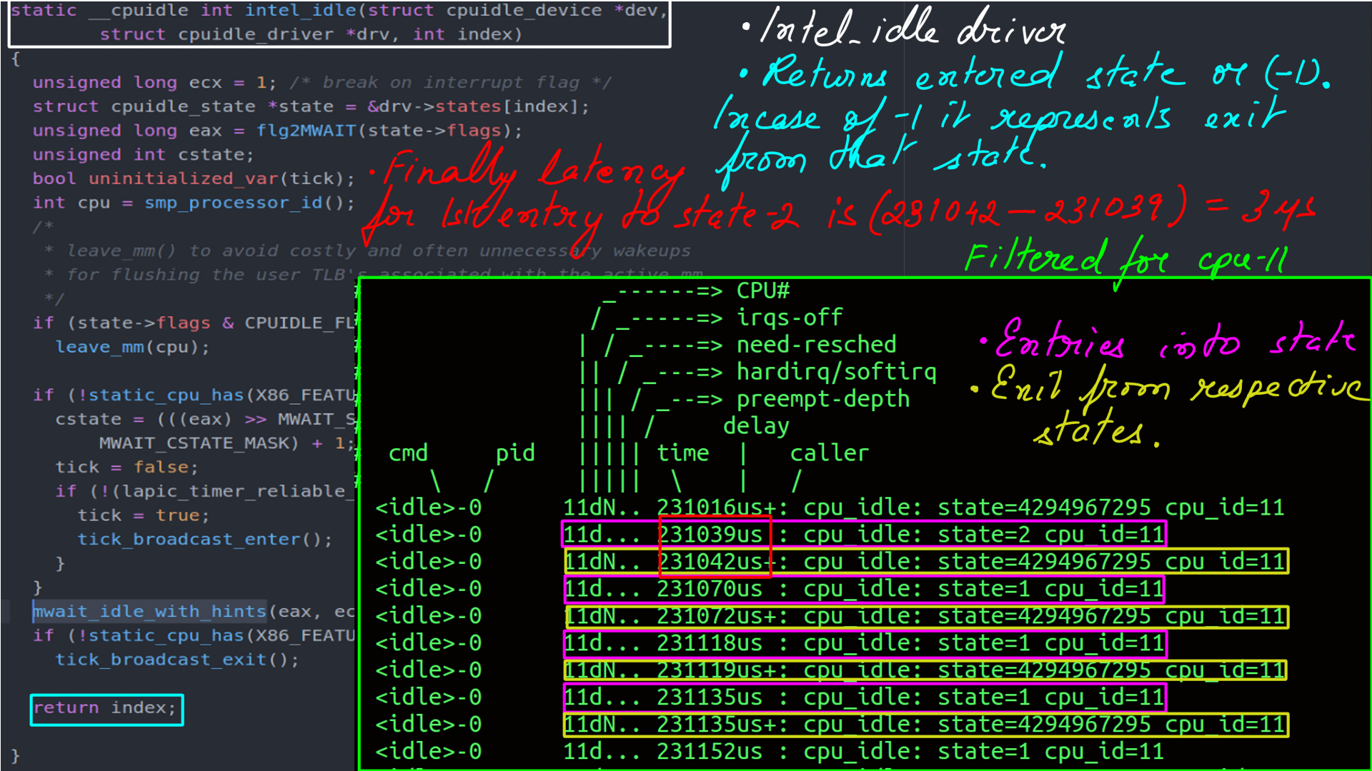
- “mwait_idle_with_hints” and __mwait are implemented in inline assembly.
static inline void mwait_idle_with_hints(unsigned long eax, unsigned long ecx)
{
if (static_cpu_has_bug(X86_BUG_MONITOR) || !current_set_polling_and_test()) {
if (static_cpu_has_bug(X86_BUG_CLFLUSH_MONITOR)) {
mb();
clflush((void *)¤t_thread_info()->flags);
mb();
}
__monitor((void *)¤t_thread_info()->flags, 0, 0);
if (!need_resched())
__mwait(eax, ecx);
}
current_clr_polling();
}
Listing-1static inline void __mwait(unsigned long eax, unsigned long ecx)
{
/* "mwait %eax, %ecx;" */
asm volatile(".byte 0x0f, 0x01, 0xc9;"
:: "a" (eax), "c" (ecx));
}
Listing-2CPUIDLE subsystem:Governor
Governor is a part of the CPUIDLE subsystem and implements the policy part. Policies can be expressed in many ways.
- One policy can be, restrict deeper idle-states for lower latency. These policies are more direct in nature.
- Others can be based on some QOS requiremment. For example, respond within a latency of a few 100 microseconds or powersave.
- Many governors may exist in a kernel but only one of them can be in control..
CPUIDLE subsystem:Gathering and undertanding latency data
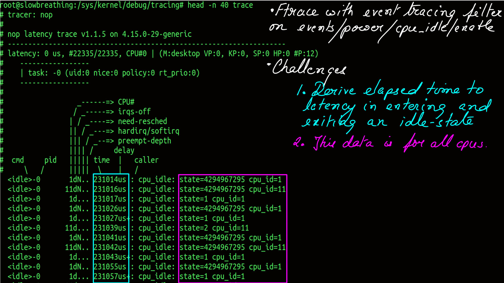
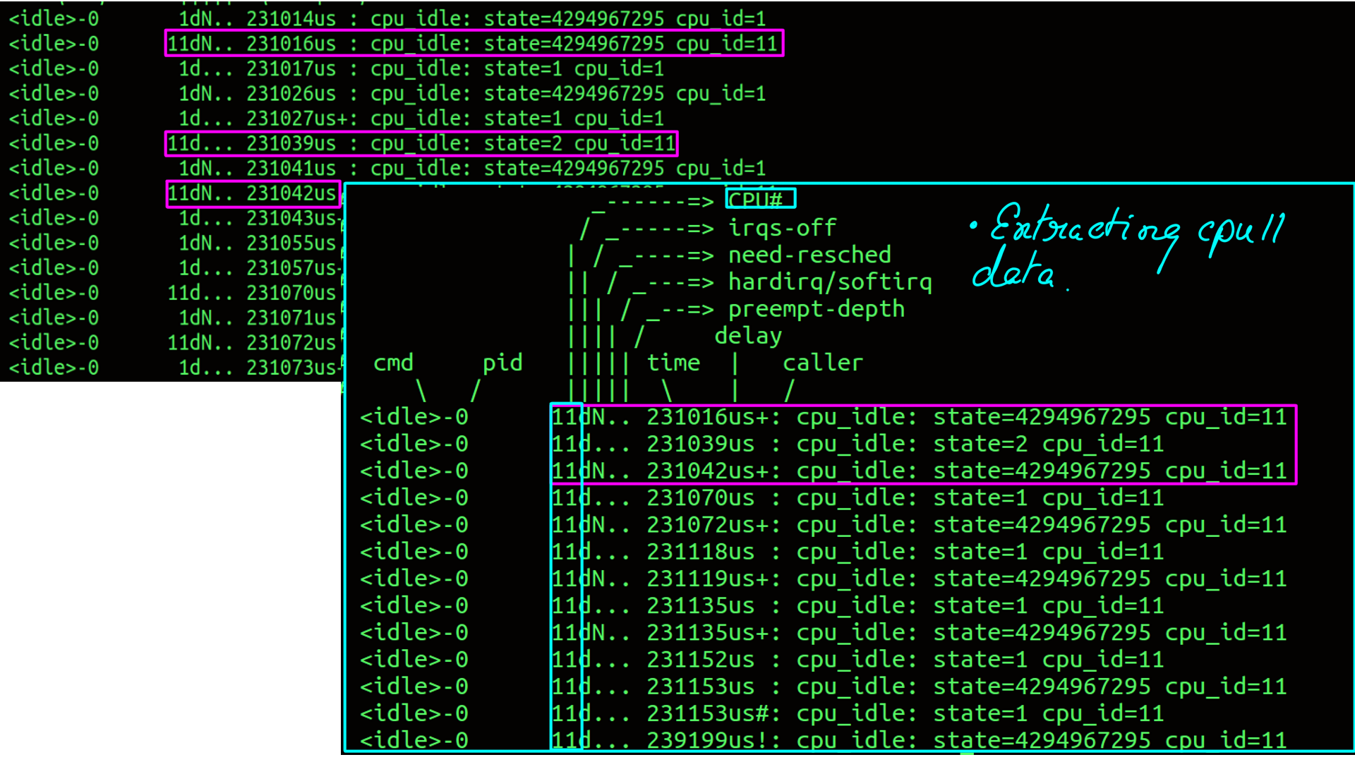
The next step is to gather and understand latency data. There are two challenges here. First, to find a tracer that can gather CPUIDLE latency data without a huge observer effect. This can be achieved by using “ftrace”. “ftrace” is the coolest tracing dude on the planet. Second, is to make sense of the data. At a very high level, what we want to understand is the impact of deep idle-states on latency.
- ftrace event tracing for cpu_idle. Which state a cpu enters and exits with respect to time lapse as duration.
- Filtered by cpu..
- What the numbers mean, and corresponding latency calculation..
- Latency by state exit and entry respectively in CSV form.
- The time series property has been retained. That will tell us if a configuration change has effected latency.
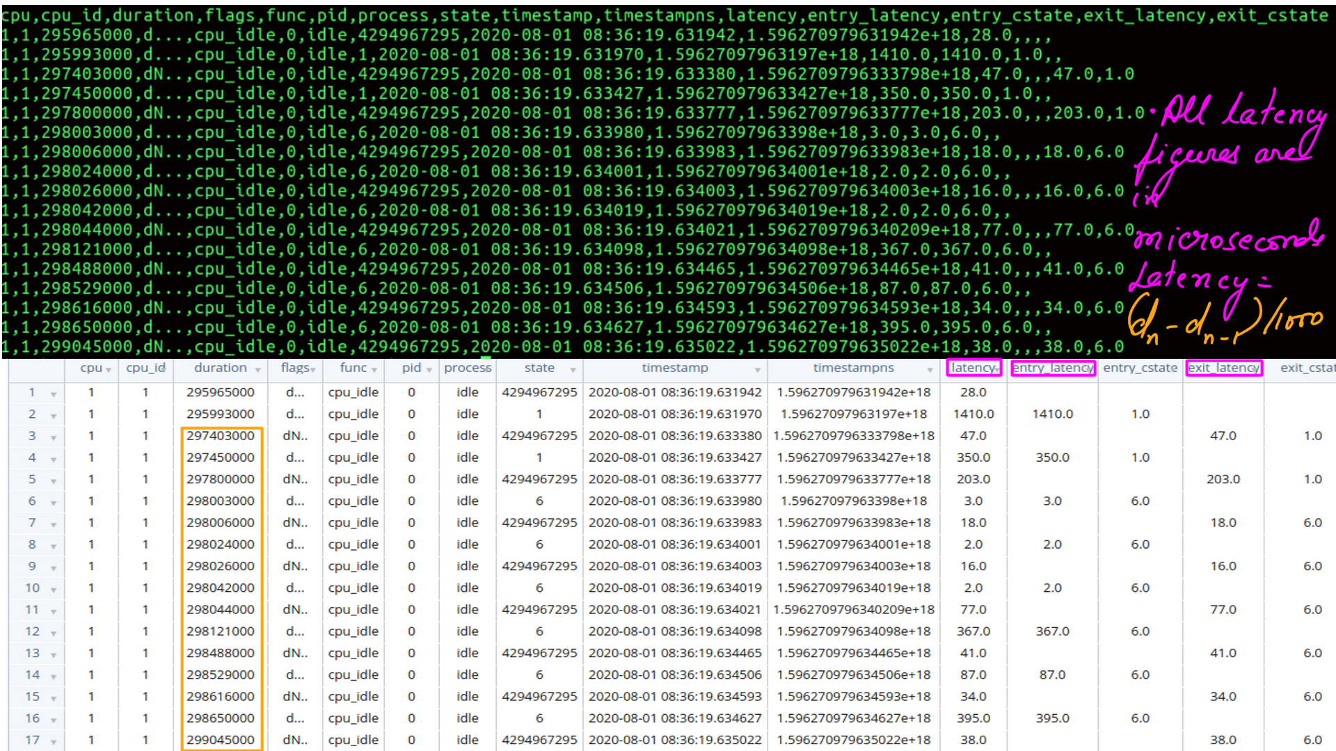
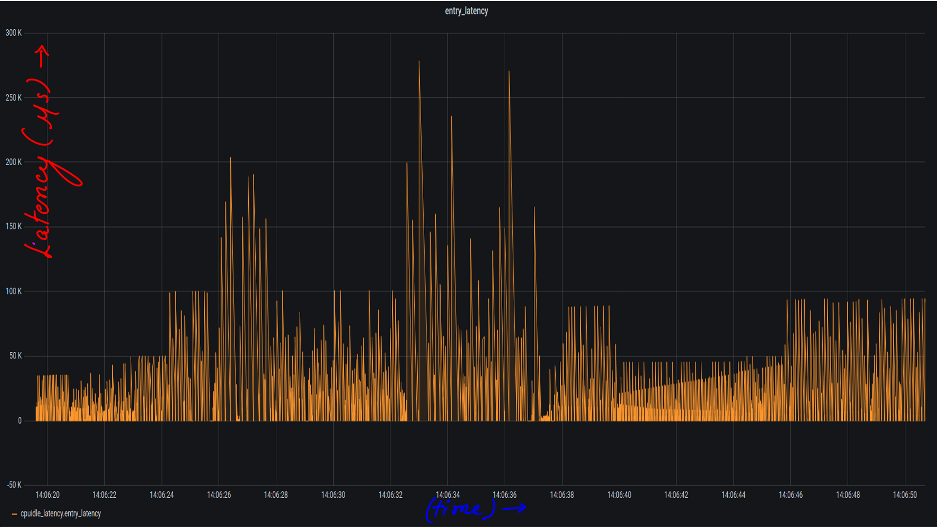
- Pushed to influxdb and then visualized by grafana..
Summary
We looked at 2 primary concepts. Firstly, a sketch of what units a CPU Core has and how it executes code and processes data. The pipeline of the core should provide a high-level idea of the flow instruction and data. Secondly, the interaction of software(Linux) with the CPU. This information is really interesting and in the field of performance absolutely indispensable. Once understood well, debugging becomes a lot easier. Fancy profilers are all very good but have a huge observer effect. ‘Ftrace’ like tools are built for this purpose. However, the data they generate may not be easily digestible. Now that we have a basic understanding, we can use these tools to measure after-effects of performance configurations in the rest of the series.
References
- What every programmer should know about memory: (This is a definitive 9 part(the links for the rest of the parts are embedded in the first one.) article on how the hardware works and, how software and data structure design can exploit it. It had a huge impact on the way I thought and still do think about design. The article first came out in 2007 but it is still relevant which is proof that basics don’t change very often.)
- Intels documenation: (Intel’s documentation is the authentic source here. But, it is incredibly difficult to read. It is as if Intel’s employees were given a raise to make it “impossible to comprehend” kind of document.)
- Agner Fog: (He benchmarks microprocessors using forward and reverse engineering techniques. My bible.)
- Linux Source: (If you are going to trace your programs/applications then having the Linux source is a must. Tracers will tell you half the story, the other half will come from here. )
- Transformer: (Modern Natural Language processing, in general, must be indebted to Transformer architecture. We however, use an asymmetric transformer setup.)
- Performer-A Sparse Transformer: (This is as cutting edge as it can get. The transformer at the heart of it is a stacked multi-headed-attention unit. As the sequences(of words or System events or stock prices or vehicle positions e.t.c.) get longer, the quadratic computation and quadratic memory for matrix cannot keep up. Performer, a Transformer architecture with attention mechanisms that scale linearly. The framework is implemented by Fast Attention Via Positive Orthogonal Random Features (FAVOR+) algorithm.)
- Ftrace: The Inner workings ( I dont think there is a better explaination of Ftrace’s inner workings.)
- Ftrace: The hidden light switch: ( This article demonstrates the tools based on Ftrace.)
- BPF: ( eBPF or just BPF is changing the way programming is done on Linux. Linux now has observability superpowers beyond most OSes. A detailed post on BPF is the need of the hour and I am planning as much. In the meantime, the attached link can be treated as a virtual BPF homepage.)