Artificial Intelligence based chip design
- Artificial Intelligence based chip design: Transformers on Chip (part-1)
- Artificial Intelligence based chip design: Chip Design (part-2)
Introduction
We have taken a traditional (TTS)Text-to-speech and (STT)Speech-to-text system and spun it on an FPGA microchip. In the pipeline of a traditional TTS system, there is a Seq-to-Seq LSTM layer rearing its “ugly latency head”. It takes approximately tens of thousands of iterations of this network to generate a second of audio.Sometimes this latency is not acceptable. Sometimes, this latency is not acceptable. Latency of these systems can be majorly attributed to the LSTMs, the technology of the day. LSTMs still have their uses, but for speech-based latency sensitive systems, they have limitations. LSTMs have played their part in the Deep Learning history and it is time for them to pass on the baton to the new King, The Transformers.
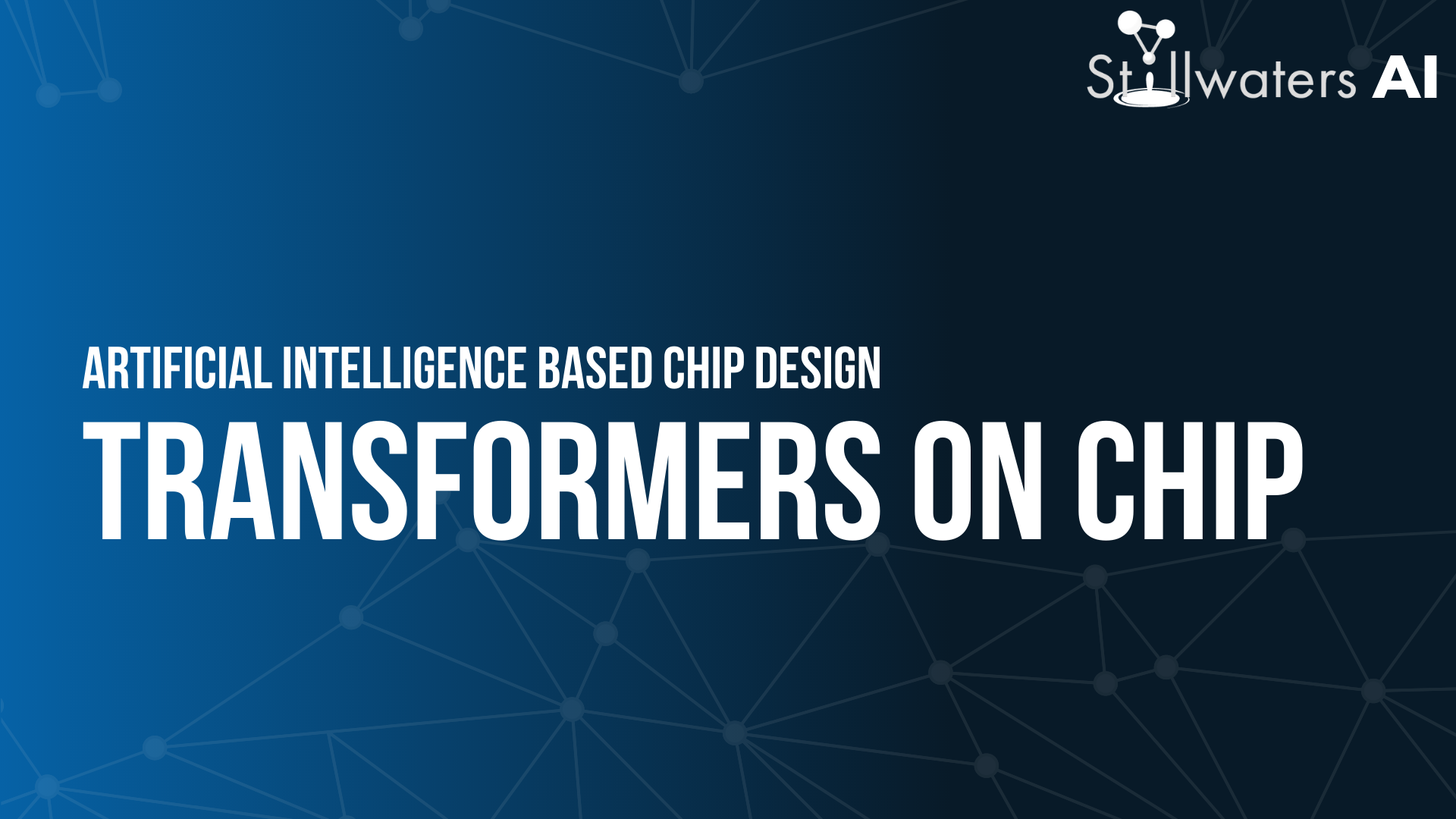
STT(Speech-to-Text)
Firstly, we took the STT based on Conformer (a transformer variant) and rewrote it using Trax.
Why Trax? Well, it has an optimizing Just-In-Time compiler for Machine learning. We have extended that for FPGA. But more on that later.
It was a huge improvement on the LSTM variant. While there was a marked improvement, it wasn’t enough. And this was running on a 2020 GPU.
Transformers are essentially ((MHSA)Multi-headed-Self-Attention) and a (FFM)feed forward Module. Both these are matrix multiplications of grand and varying scale. The Conformer has an additional CM(Convolutional Module) which is a matrix filter operation.
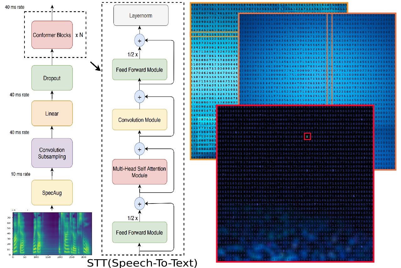
TTS(Text-to-Speech)
Secondly, we took the TTS based on the transformer and did exactly the same. Again it was a decent improvement on the LSTM version. But, not enough. Again, this was running on a 2020 GPU.
GPUs are great at handling the “grand” part despite some transformers having billions to even trillions of parameters.
- The “varying” part is proving extremely tricky for GPUs. Both MHSA and FFM have varying parallelism requirements(from one model to another).
- Also, the standard precision leads to lots of wastage energy. GPU’s SIMD/SIMT lock-step style execution model makes matters worse. Lock step style execution is prohibitive in terms of energy wastage.
- Last but not least, the extra control structure on the GPU is not useful(wasteful) for matrix multiplication. GPU is a general-purpose device and for something as specific as tuning a massive matrix multiplication it is found wanting. It is not a natural fit would be the right phrase.
- All of the above contribute to tons of electricity, produce a lot of heat, and use fans for cooling.
- And a large number of environments where we apply deep learning like speech devices, self-driving cars, production lines, etc, are not agreeable to it.
- This also makes the maintenance and life expectancy of a GPU an issue.
FPGAs as modern digital ShapeShifters
The CPUs and especially GPUs are nearing their transistor limit. The world is moving toward specialized hardware to meet the exponentially growing demand for computers:
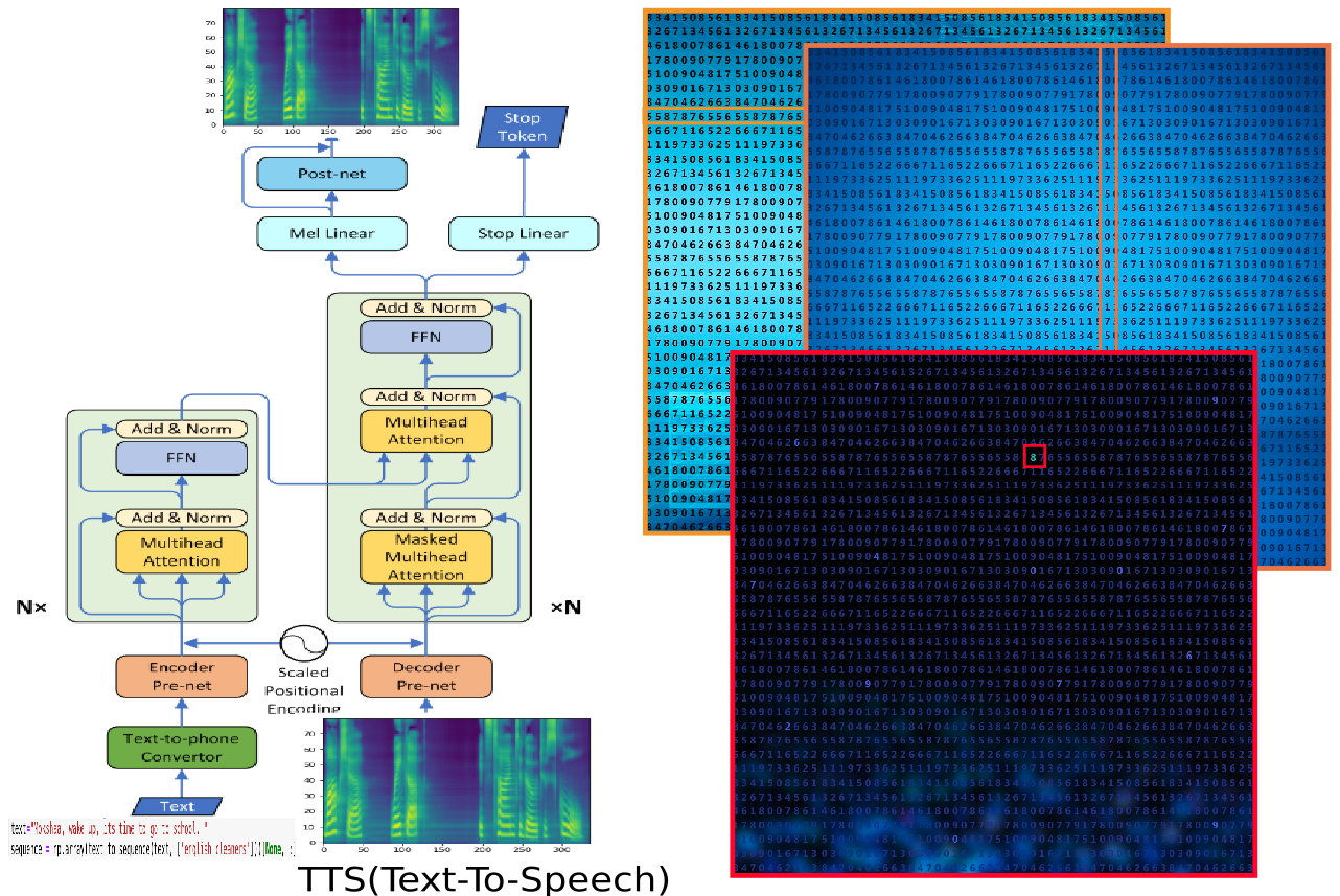
- Field-programmable gate arrays (FPGAs) are reconfigurable computer chips that can be programmed to implement any digital hardware circuit.
- FPGAs consist of an array of different types of programmable blocks (logic, IO, and others) that can be flexibly interconnected using prefabricated routing tracks with programmable switches between them.
- The bit-level reconfigurability of FPGAs enables implementation of the exact hardware needed for each application (e.g. datapath bit-width, pipeline stages, number of parallel compute units, memory subsystem, etc.) instead of the fixed one-size-fits-all architecture of CPUs or GPUs.
- Consequently, they can achieve higher efficiency than CPUs or GPUs by implementing instruction-free streaming hardware
- FPGA-RAM
- An FPGA BRAM(BlockRAM) consists of an SRAM-based memory core, with additional peripheral circuitry to make them more configurable for multiple purposes and to connect them to the programmable routing FPGA vendors can add circuitry that allows designers to repurpose the LUTs(Look Up Tables) that form the logic fabric into additional RAM blocks.
- DSP Blocks
- With the prevalence of multipliers in FPGA designs from key application domains, and their lower area/delay/power efficiency when implemented in soft logic, they quickly became a candidate for hardening as dedicated circuits in FPGA architectures.
Optimizing on Hardware Accelerator
The idea here is to hardware accelerate the huge matrix multiplication which is the core of Transformers. Given the size of the matrices in transformers ( a few billion parameters in 2020), there is practically no chance of them fitting inside a top end FPGA board, not for at least the next decade. So the trick is to chop these huge matrices being multiplied into smaller tiles and reuse these tiles as much as possible before moving on to the next tile. One of the oldest tricks in a new Avatar.
There are 4 key points of FPGA Hardware Optimization
- Play to FPGAs strength, no extra control logic
- Minimize access to OFF-chip RAM by having multi level on chip buffer made of BRAM and LUTRAM
- Maximize the compute parallelism (PE)ProcessingElements
- And the most vital, balance the above 2.
- PEs must be well fed and not starving
- Balance cached data with streaming( weights(Mul1) may be cached more and the input will be streamed more(Mul2))
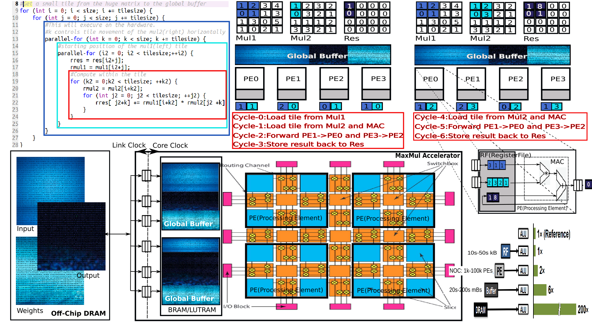
Optimizing on Hardware Accelerator(MAC Style)
The hardware mapping is the most fabulous part carried out by our mapper. It takes the code below and unrolls the MaxMul loop into the Hardware.
- There are 2 Styles
- MAC Style(Multiply Accumulator)
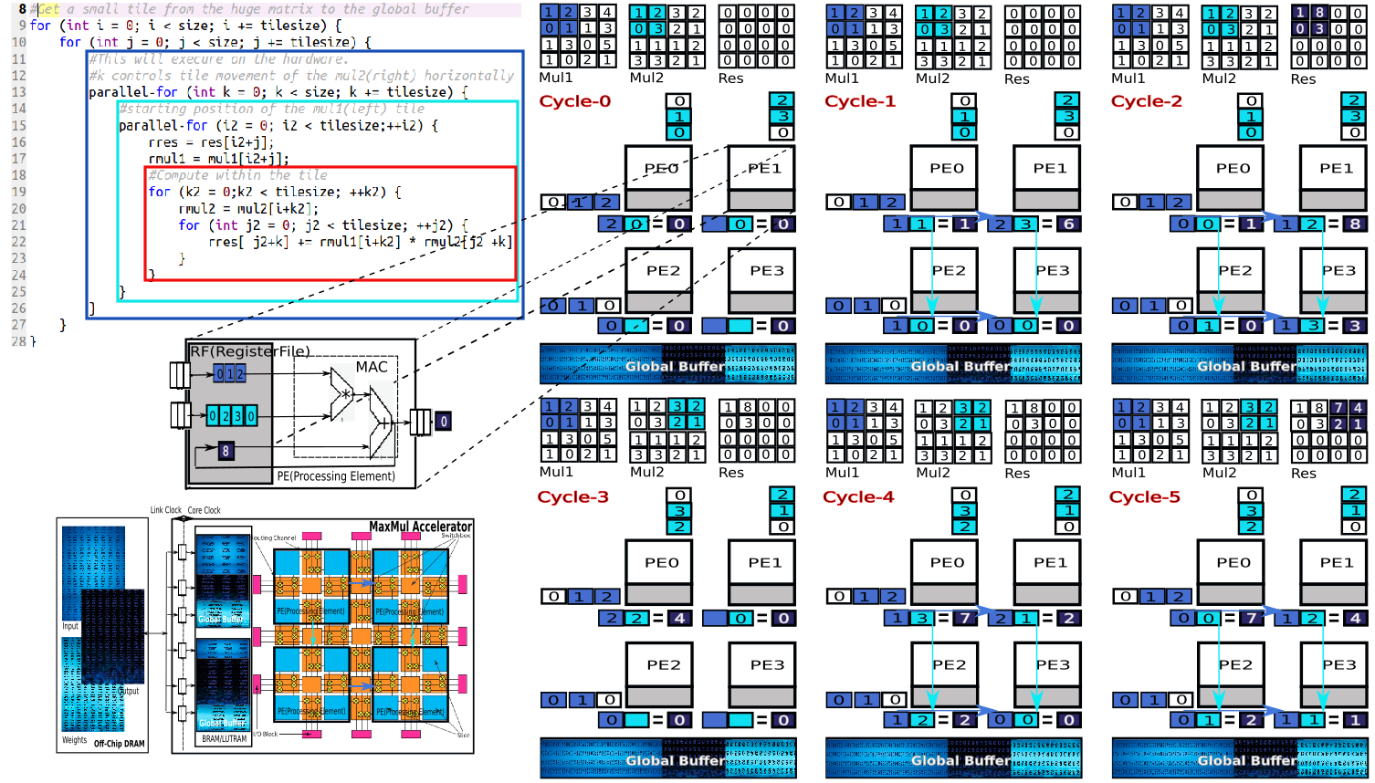
- For a 4X4 matrix a 2X2 PE array as shown will take 24 cycles give or take.
- For a 4X4 matrix a 4X4 PE array as shown will take 6 cycles give or take.
- SA Style (Systolic Array)
- For a 4X4 matrix a 2X2 PE array as shown will take 24 cycles give or take.
- For a 4X4 matrix a 4X4 PE array as shown will take 6 cycles give or take.
- We retrofit this mapper to trax.
Optimizing on Hardware Accelerator(Systolic Array Style)
Same as above except the microarchitecture uses systolic array design with The PEs being pipelined. Follow the color coding especially the data movement(light and dark blue boxes and arrows) into the PEs(Processing Elements) and data forwarding among PEs. The NOC(Network On Chip) architecture which is not shown, is slightly different for both the MAC Style(Multiply Accumulator) and the SA Style (Systolic Array).
Variables in the design
The SA Style (Systolic Array) works better for bigger tiles when it’s pipelines are fully fed for longer durations. But not too big as the NOC feeding the buffers has its own limitations. The size of the tile and indeed the style of the microarchitecture( MAC or SA) are one of the many design variables that need to be configured for best results. These in turn depend on quite a few more design variables, some of them are due to software constraints (Matrix size etc.) and others are hardware constraints (BRAM etc). Here are a few important design variables.
- The SGB(size of Global Buffer) based on available BRAM and LUTRAM.
- More LUTRAM would mean bigger buffers, better reuse, but fewer PEs and lesser parallelism.
- The LGB(Layout(Locality) of GLobal Buffer)
- The size of the MT (Matrix Tile) and PET(PE Tile)
- The size of RF(RegisterFile)
- As a general rule, bigger/multi-level caching(SGB/NOC/RF are like L3/L2/L1) would better lookup performance but increase data replication and eat into logic space(PEs)
- The layout of NOC(Network on Chip)
- With 100s of MBs to 1000 GBs of matrix sizes to choose from in modern transformers, myriad different Accelerator boards, Shape shifting configuration options on these boards, all the above variables to choose from, the configuration space is a serious problem of plenty.
- A general configuration done by a domain expert(on Transformers and FPGA board) will give us decent improvement over a software only implementation but, nowhere near what the hardware is capable of unless the configurations are done by either Ramanujam or Tesla(Only these 2, others were normal).
Summary
Migrating compute that requires extreme parallelism, or compute that can benefit from custom data path or precision should be moved to FPGA chips. Infact this is FPGA’s backyard. The overall throughput can be a few hundred times better. Latency can be a bit tricky, but still can be a lot better with the flexibility that FPGA chips offer.
References
- What every programmer should know about memory: (This is a definitive 9 part(the links for the rest of the parts are embedded in the first one.) article on how the hardware works and, how software and data structure design can exploit it. It had a huge impact on the way I thought and still do think about design. The article first came out in 2007 but it is still relevant which is proof that basics don’t change very often.)