Artificial Intelligence based chip design
- Artificial Intelligence based chip design: Transformers on Chip (part-1)
- Artificial Intelligence based chip design: Chip Design (part-2)
Introduction
In part-2 we treat the resources on FPGA chips, Workload, other design parameters as design variables. Finally, we feed the design variables into the Deep Reinforcement Learning agent to learn, and then suggest optimal placement of blocks to maximize certain goals like latency, etc. This part describes a few of the hardware variables and how to co-express the software and hardware variables that share a complex relationship. This co-expression is vital. For example, reducing bit width costs accuracy but frees up hardware resources that could be used for compute or cache. The Deep Reinforcement Learning Algorithm is supposed to figure out a balance that speeds up computation for tolerable accuracy losses(if at all). To use a boxing term, pound for pound, the same hardware micro-designed by a Deep Reinforcement Learning Agent for carrying a specific load.
Chip Design: Layout, Locality and Resource Allocation
Although current FPGA accelerators have demonstrated better performance over generic processors for specific workloads, the accelerator design space has not been well exploited. One critical problem is that the computation throughput may not well match the memory bandwidth provided by FPGA platforms.
But the bigger issue is Hardware design or even certain elements in it are usually not a variable in application design. Hardware design is a bubble, and so is software design but these don’t meet. There is a case to be made for hardware and software co-design. But a few more hardware-specific design variables first.
- Matrix Sparsity(MS) is known to cost a lot. Checks can be built into the PE to reduce the overall cache requirement, but it comes at the cost of chip fabric space and end-to-end latency. It’s a classic trade-off.
- Reducing Bit Width(BW) costs accuracy
- Recent developments point toward next-generation Deep Learning algorithms that exploit extremely compact data types (e.g., 1bit, 2bit, 4bit, 8bit, 12bit, etc.).
- This is FPGAs’ backyard but was never done dynamically and as a whole with software in the loop.
Deep Reinforcement Learning Agent
With so many design variables identified above, this essentially is a deep search problem. Many of these design variables can assume millions to billions of values and the combinatorial space is practically impossible to go through with an exhaustive search policy. Last but not least, the entire argument for Artificial Intelligence is generalization, which is the whole point of the Design Variables.
Our Rules of the Game
Essentially these are the boundary conditions asserted by the design and/or inherent in the chip. Add to that the design variables and we have the complete rules of the game.
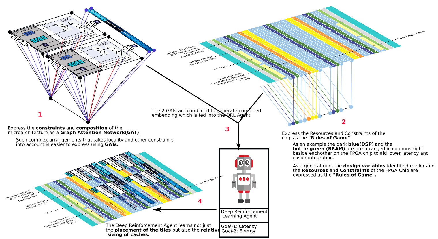
- Express the constraints and composition of the microarchitecture as a GAT(Graph Attention Network)
- Such complex arrangements that take locality, composition, arrangement, and other constraints into account are easier to express using GATs. Our current implementation is custom but for the next iteration, we’d like to use the graph neural network.
- Express the Resources and Constraints of the FPGA Chip as the “Rules of the Game(Alphago Zero learned the game of go from scratch, with the rules of GO as boundary constraints)”
- As an example, the dark blue(DSP) and the bottle green (BRAM) are pre-arranged in columns right beside each other on the FPGA chip to aid lower latency and easier integration.
- The logic fabric(FPGA fabric) can be used in compute or as RAM(LUTRAM). Both Altera/Intel and Xilinx have elected to make only half of their logic blocks LUT-RAM capable in their recent architectures. This is another “rule of the game”. Similar to chinese chess, where a piece is captured and reprogrammed rather than removed from the board. A little like saying if you are not logic you are ram. And the Deep Reinforcement Learning Agent is expected to learn it over multiple training iterations.
- As a general rule, the design variables identified earlier and the Resources and Constraints of the FPGA Chip are expressed as the “Rules of Game”.
- We generate combined embeddings that are fed into the Deep Reinforcement Learning Agent for Training.
- The Deep Reinforcement Agent with multiple training iterations learns not just the placement of the tiles but also the relative sizing of caches and indeed the values of the design variables identified above.
- It goes without saying that the prediction for most design variables more than satisfies the primary goal(latency) and shatters the secondary goal(energy) and tertiary goal(throughput).
- But the result is fascinating for a completely different reason. This is the beginning of a recipe for the future of chip design.
Summary
What started as an experiment led to something as fascinating as this was something beyond expectation at the beginning. Now that it has, it can be extended to all kinds of FPGA chips and beyond. The idea of “AI Accelerator” is not new but placing it in the same design bubble as the AI software has advantages not exploited earlier to the best of my knowledge. This is how we exploit the limits of the hardware. Specialized, purpose-built chips are set to become commonplace, not at the cost of general-purpose chips though. Deep Reinforcement Learning has been a revelation. I feel in the chip design and similar domains this is a technique that is severely underexploited.
Future
This is the first iteration, and the rush to the finish line hurried us up. The future looks mouthwatering and majorly because of the tech we had to leave out for this iteration. Here are a few.
- The modern FPGA ditches the traditional DSPs for tensor blocks that are purpose-built for Deep Learning.
- Processing near memory is moving compute to memory literally. Processing-in-memory architectures propose moving the compute into the memory that literally stores the weight matrix. Processing in memory architectures can also increase the memory bandwidth, as the number of weights that can be accessed in parallel is no longer limited by the memory interface.
References
- What every programmer should know about memory: (This is a definitive 9 part(the links for the rest of the parts are embedded in the first one.) article on how the hardware works and, how software and data structure design can exploit it. It had a huge impact on the way I thought and still do think about design. The article first came out in 2007 but it is still relevant which is proof that basics don’t change very often.)